pcb layout engineer training Pcb training with placement in chennai by alexander sam
If you are looking for PCB Training - Day 3 - EasyEDA open source hardware lab you've visit to the right page. We have 10 Pictures about PCB Training - Day 3 - EasyEDA open source hardware lab like Pcb Layout Engineer Stock Video Footage - 4K and HD Video Clips, PCB Layout Services| PCB Prototype | Reverse Engineering and also Advanced PCB Layout Course. Here it is:
PCB Training - Day 3 - EasyEDA Open Source Hardware Lab
 oshwlab.com
Pcb Design Engineer Resume Pcb Design Engineer Resume Samples Pcb
 pcbhouses.pages.dev
Pcb Design Training - Pcb Design School
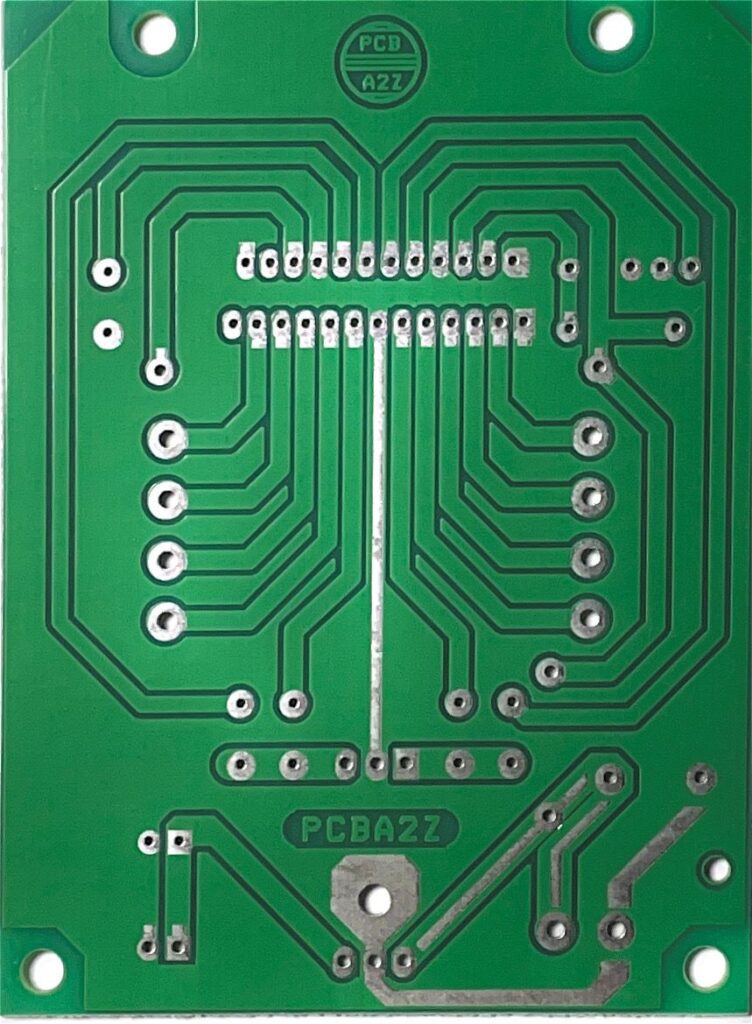 pcba2z.com
Pcb Layout Engineer Stock Video Footage - 4K And HD Video Clips
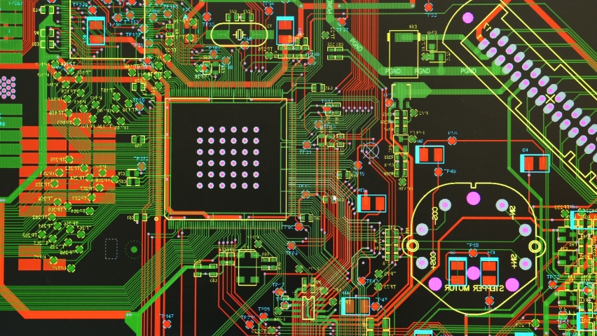 www.shutterstock.com
Advanced PCB Layout Course
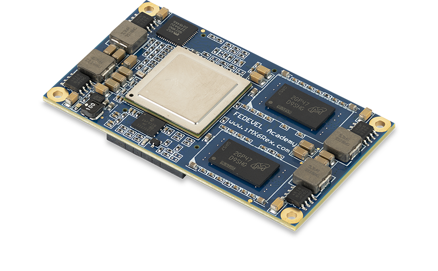 www.fedevel.com
PCB Layout Services| PCB Prototype | Reverse Engineering
 gespcb.com
PCB Design Course And Training – Pramura
 www.pramura.com
Pcb Design Training - Pcb Design School
 pcba2z.com
PCB Training With Placement In Chennai By Alexander Sam - Issuu
 issuu.com
Learning PCB Design - C2workspace.tech
 c2workspace.tech
Pcb layout services| pcb prototype. Pcb layout engineer stock video footage. Pcb design training
